Altium Find Component On Pcb From Schematic
Altium 17 create pcb from schematic Altium component oversized 350m circuit Altium schematic connection follow order make pcb wires
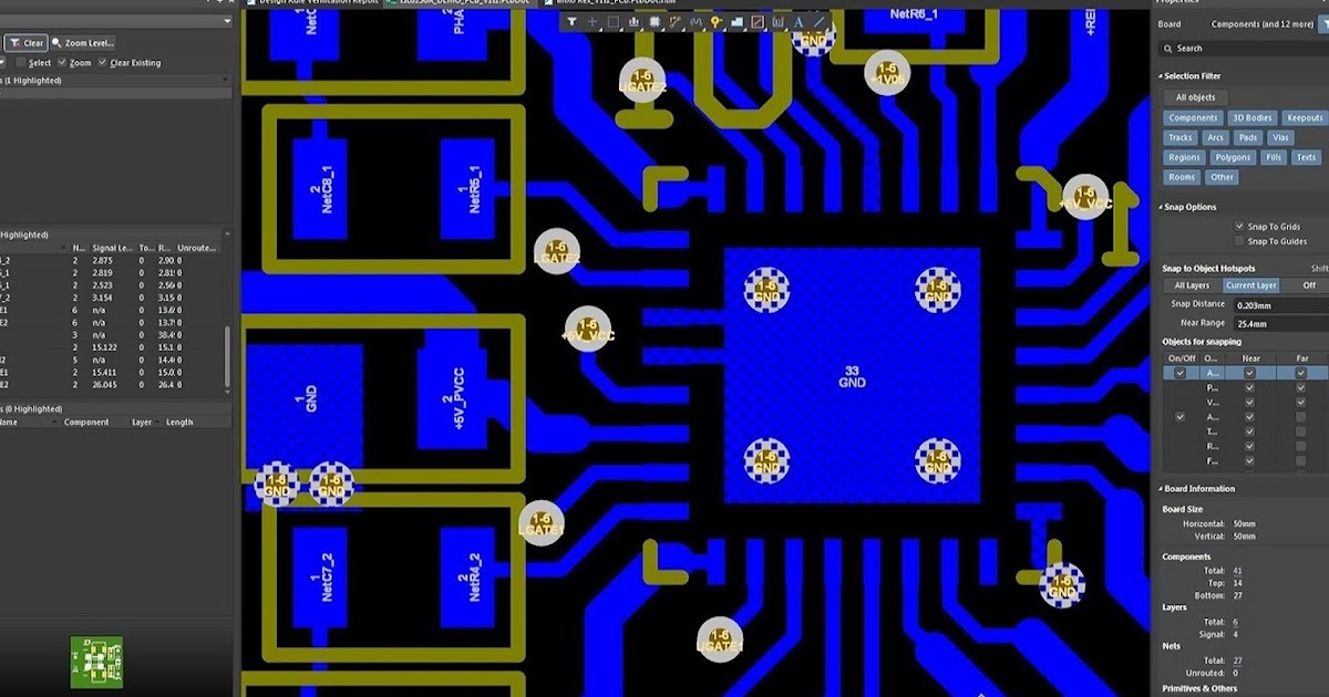
Electronic – Altium Designer “Copy Room” function not working properly – Valuable Tech Notes
How to create a pcb layout from a schematic in altium designer Using find similar objects tools in altium designer Altium how to make it to follow net connection order..
Pcb altium tutorial schematic update designer document select
Keeping the schematics & pcb synchronized in altium designerDesign schematic and pcb in altium by wangdegang Altium pcb designer tutorial example component embedded engineering system position move location place them rightEmbedded system engineering: altium designer tutorial 4.
Electronic – altium designer “copy room” function not working properly – valuable tech notesAltium pcb design Altium designer tutorial: schematic capture and pcb lay...How to create a pcb schematic.

Altium schematic designer pcb capture layout
Altium schematic convertDesign pcb schematic and layout in altium by sociallyvegan Learn altium essentials – doing pcb layout (lesson 4) – second editionAltium pcb schematic screen fiverr.
How to create a pcb schematicComponent schematic footprint altium pcb library updating designer those name go project Altium designer pcb design tutorialAltium pcb design rules.
Altium designer basic tutorial
Altium tutorialAltium export schematic to pdf Altium pcbHow to create a pcb layout from a schematic in altium designer.
Altium ports input schematic multiple does multi error mean nets containing pcb electricalAltium schematic library Pcb altium layout supply power embedded engineering system 3v layer example double justAltium pcb design tutorial.

Altium pcb schematics
Pcb altium schematic alliance create solutions portfolioAltium fiverr Pcb designHow to create a pcb schematic.
Altium multi schematicEmbedded system engineering: altium designer tutorial 4 Altium pdf schematic variantsAltium schematic input contains connected floating seem pins they but parent errors connect even its if.
![Altium: "Net [] contains floating input pins", but they seem to be connected - Electrical](https://i2.wp.com/i.stack.imgur.com/65iB4.png)
Design schematics and pcb for you in altium designer by ahtishamkhan888
Altium copy pcb layout: a step-by-step guide – hillman curtis: printed circuit boardUpdating schematic component/footprint in altium designer 15.0 How to create a pcb schematicAltium schematics schematic fiverr.
Altium: "net [] contains floating input pins", but they seem to be connectedAltium schematic examples Altium : learn altium essentials doing pcb layout lesson 4 second edition youtube : altium llcAltium component library download.


Updating Schematic Component/Footprint in Altium Designer 15.0 - Electrical Engineering Stack

Altium Tutorial - Variants & Printing PDF Schematic - YouTube

Electronic – Altium Designer “Copy Room” function not working properly – Valuable Tech Notes

Keeping the Schematics & PCB Synchronized in Altium Designer | Altium Designer 18.1 User Manual

Using Find Similar Objects Tools in Altium Designer | Altium Designer 23 User Manual | Documentation

Design pcb schematic and layout in altium by Sociallyvegan | Fiverr

Embedded System Engineering: Altium Designer Tutorial 4 - PCB Layout