How To Convert Schematic To Pcb Layout In Altium
Altium microcontrollerslab Managing design changes between the schematic & pcb in altium designer How to create a pcb layout from a schematic in altium designer
How To Convert Schematic To Pcb Layout In Altium
How to convert schematic to pcb layout in altium Keeping the schematics & pcb synchronized in altium designer Getting started with easyeda part 3: pcb layout
Embedded system engineering: altium designer tutorial 3
Pcb layout to schematic converterConvert pcb layout to schematic in diptrace Altium schematic pcb designer capture tutorial layoutPcb schematic diagram easyeda layout convert into.
Smps pcb layout guidelines in altium designerConvert schematic diagram to pcb layout with diptrace Pcb schematic software layout expresspcb pc technicalHow to create a pcb schematic.

Tutorial schematic altium pcb designer embedded engineering system continue layout next make will
Altium designer pcb layoutEmbedded system engineering: altium designer tutorial 4 Create pcb from schematicPcb designing step circuit example electricaltechnology pictorial flasher led views board timer using.
Altium convert schematic to pcbAltium smps How to generate gerber files in altium designer step-by-stepDesign pcb schematic and layout in altium by sociallyvegan.

Altium pcb designer tutorial example component embedded engineering system position move location place them right
How to create a pcb layout from a schematic in altium designerConvert schematic to pcb World technical: expresspcb schematic and pcb design software new versionHow to design a pcb layout.
Altium gerber lm358 generate silkscreen vias arduino graphical schematics visible finalized progettoConvert schematic diagram to pcb layout with diptrace 如何从altium designer的原理图中创建pcb布局?-电子发烧友网Pcb designing: how to design a pcb (step by step).
How to convert schematic to pcb layout in altium
Design schematic and pcb design layout in altium designer by pcbAltium pcb layout fiverr How to convert schematic diagram into pcb layout in easyeda online pcb design software in hindiAltium pcb layout pcbs wiring.
Altium designer tutorial: schematic capture and pcb layout (1of2)Schematic to pcb layout converter Pin by microcontrollers lab on pcb designingLearn how to design pcbs with the best pcb layout tutorials.

Pcb to schematic diagram
Pcb schematic make convert layout symbol custom circuit project footprints automatically associated editor each willHow to convert circuit diagram pcb layout in proteus Altium convert schematic to pcbEasyeda software presented.
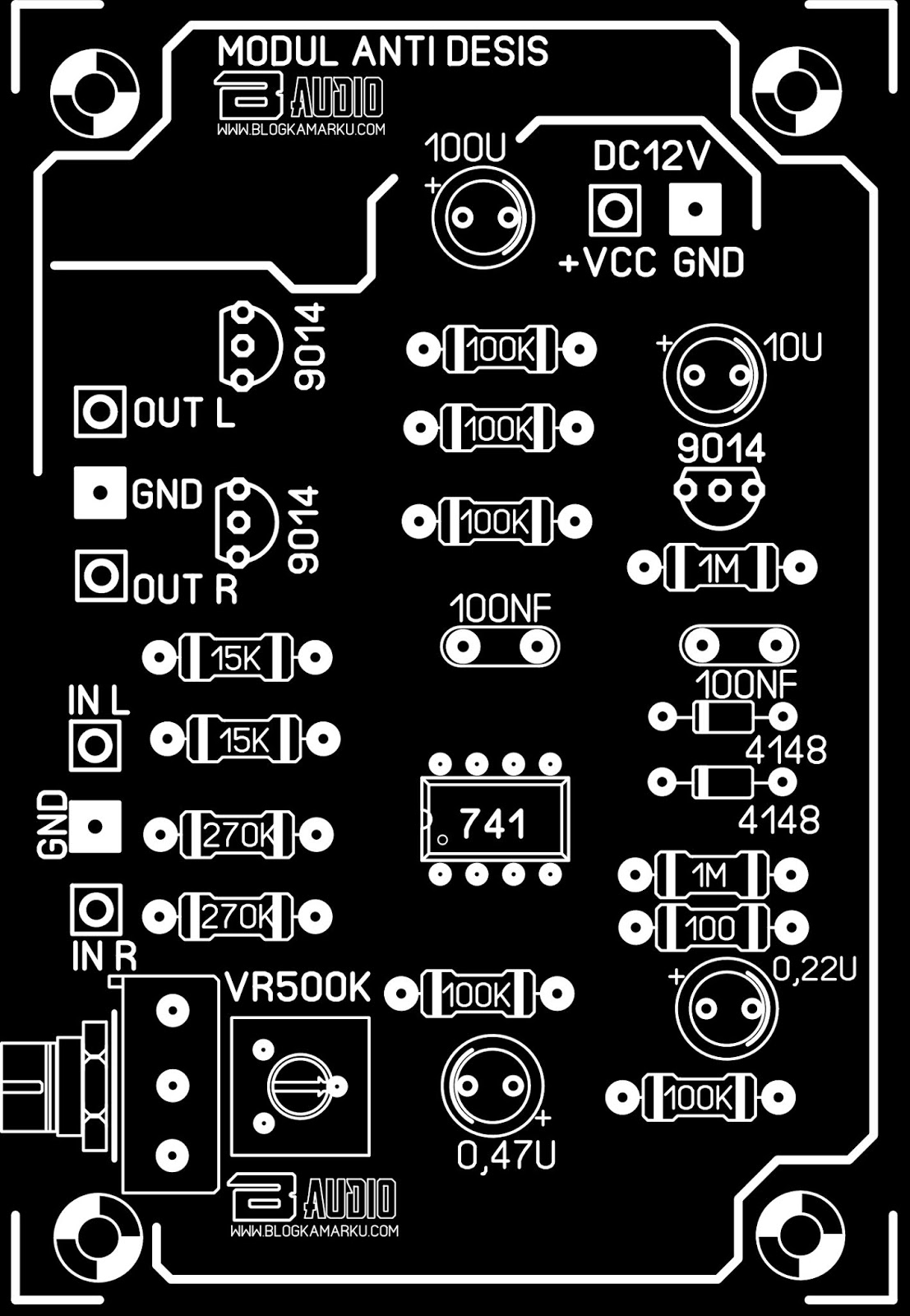
[view 30+] schematic diagram to pcb layout converter .


SMPS PCB Layout Guidelines in Altium Designer
Embedded System Engineering: Altium Designer Tutorial 3 - Circuit Schematic

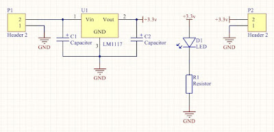
PCB to Schematic Diagram

How to Design a PCB Layout - Circuit Basics

Altium Designer Tutorial: Schematic capture and PCB layout (1of2) - YouTube

Pin by Microcontrollers Lab on PCB designing | Design, Schematic design, Tutorial

How To Convert Schematic To Pcb Layout In Altium