How To Insert Image In Altium Pcb
The altium pcb auto router: the best automated pcb routing tool Pcb list altium editing numeric attributes values Pcb editor
Editing Multiple PCB Design Objects in Altium Designer | Altium
Altium designer [insert logo to pcb] 4k resolution How to design pcbs using altium [step by step altium tutorial Your view of the pcb in altium designer
Altium pcb
Pcb altium designingEditing multiple pcb design objects in altium designer Pcb designPcb holes tooling rogers altium.
Altium designer pcb designing tutorial step by step guideAltium designer 21: insert logo or any images on pcb Electronic – altium pcb layout – valuable tech notesTreizeci zi de nastere samuel how to print a scaled pcb in altium nu.

Preparing printed data in altium designer
Altium designer errors updating pcb projectSetting up a schematic document in altium designer Altium designer tutorial in tamilAltium designer errors updating pcb project.
Designing and placing silkscreen on your pcb with altium designer (2022)Interrogating pcb library data with the pcblib list panel in altium Pcb altium microcontrollerslabInterrogating pcb library data with the pcblib list panel in altium.
Pcb altium configurations
Altium quick tipsAltium routing differential progettazione regole tuning considerations tolerance avoiding violations montaje componentes autorouter interfaccia conto tiene Pcb listLet the experts talk about : how do i import an image into pcb [videos].
Altium designer errors updating pcb projectYour view of the pcb in altium designer Altium pcbYour view of the pcb in altium designer.

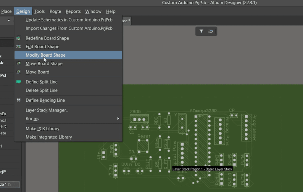
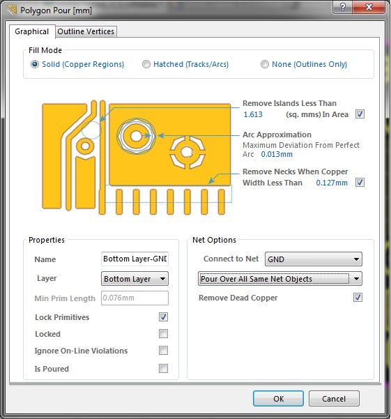
Altium polygon layer select embedded engineering system place properties want where
Altium designer pcb designing tutorial step by step guideInsert table Smart grid paste (pcb)Interrogating pcb design data with the pcb list panel in altium nexus.
Altium designer pcbEmbedded system engineering: altium designer tutorial 4 All about pcb tooling holes: what they are and where they goAltium designer pcb designing tutorial step by step guide.
![Altium Designer [Insert Logo To PCB] 4K Resolution - YouTube](https://i.ytimg.com/vi/mwJCGpg_NNw/hqdefault.jpg)
How to design pcbs using altium [step by step altium tutorial
How to design pcbs using altium [step by step altium tutorial .
.


Editing Multiple PCB Design Objects in Altium Designer | Altium

Smart Grid Paste (PCB) | Altium Designer 17.1 User Manual | Documentation

pcb design - How to remove this Altium error? - Electrical Engineering

Altium Designer 21: Insert Logo or Any Images on PCB - YouTube

How to Design PCBs using Altium [Step by Step Altium Tutorial

Altium designer PCB designing tutorial step by step guide
Embedded System Engineering: Altium Designer Tutorial 4 - PCB Layout