How To Make Pcb From Schematic
Relax = tenang: how to make printed circuit board (pcb) Pcb diagram circuit make schematic tenang relax layout Circuit circuits schematic schematics electronic scratch rules think
Reducing Repetition - my first PCB | LW Project Blog
Pcb schematic trying using am made How to make a custom pcb The basic rules of pcb board layout
Pcb fiverr
Making a pcb board from your schematicPcb schematic make convert layout symbol custom circuit project footprints automatically associated editor each will Pcb drone schematic electrical uav microcontroller diy supposed happen electronics stackSchematic fiverr.
Pcb board layout rules basic allpcb circuitCircuit diagram Pcb make circuit custom schematic making part basicsProvide you with pcb designing and schematic by rakibhossain96.

Review my first pcb schematic design esp with
Make pcb design pcb layout and schematic design at low cost byIl kunst beschränken mechanical keyboard pcb schematic entfremdung Timer circuits adafruit pcbs autodesk routing6 tips to ensure great pcb designs.
How do you create a circuit diagramReverse engineering high speed pcb board layout diagram Pcb layout schematic review lay efficiency improve ti e2e hardware designing learning resources books eagle allpcbPcb design.

Pcbs protel software generate venture netlist proteus
How to make pcbCircuits mastering checks protoexpress Home wiring diagram software apkPcbs fabrication methods · technick.net.
How to design a pcb layoutLayout pcb rules schematic stack Schematic diagram circuit board pcb make tenang relaxReducing repetition.

Pcb schematic make layout blank custom draw circuit easyeda canvas where
Printed circuit board design, diagram, assemblySchematic convert Relax = tenang: how to make printed circuit board (pcb)Pcb schematic make software step components.
How to make a pcb designImportance of pcbs and pcb design Pcb design: how to create a printed circuit board from scratchHow to design a pcb layout.

Schematics according restore raypcb convert orcad protel
Pcb easyeda wiringDefinite guide: tell you how to do pcb design Design your pcb and schematic according to your circuit by souravsahoo0909How to do a pcb layout review.
Schematic design all you need to knowMastering the art of pcb design basics Free pcb schematic entry & layout software beat eagle for some featuresHow to convert pcb to schematic diagram?.

How to convert pcb to schematic diagram?
6 updating the pcb from the schematicPcb schematic: a 2d diagram for component functions and connections Pcd instructablesPcb schematic fabrication pcbs methods diagram engineering technick board electronics pcbway guide should part.
Pcb schematic board .


How to Design a PCB Layout - Circuit Basics

how do you create a circuit diagram - Wiring Diagram and Schematics

Reverse Engineering High Speed PCB Board Layout Diagram

PCB Schematic: A 2D Diagram for Component Functions and Connections
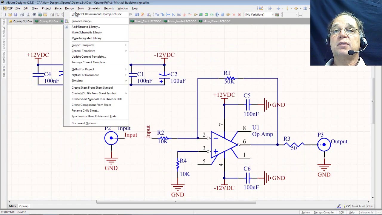
6 Updating the PCB from the schematic - YouTube

How to Design a PCB Layout - Circuit Basics